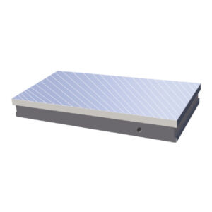
Overview of Halbach Arrays (2D) & Magnetic Chucks
Achieve superior magnetic field uniformity and holding force with our engineered Planar Halbach Arrays.
Arrange permanent magnets in a 2D pattern.
Often a ‘checkerboard’ or discrete multi-pole layout.
We superimpose the magnetic flux onto a single active face while shielding the mounting side.
This ‘one-sided flux’ technology is critical for applications that require:
– High-efficiency sputtering magnetrons
– Semiconductor wafer clamping
– Plasma confinement, and levitation platforms.
Standard magnetic plates waste energy on the back iron.
Our planar arrays deliver up to 40% higher flux density at the working surface.
We specialize in the complex assembly of these multi-axis repulsion grids.
They deliver large-scale planar arrays with exceptional flatness and field homogeneity.
Engineering & Manufacturing Capabilities
Complex 2D Matrix Assembly:
Assembling a 2D Halbach grid involves managing repulsion forces in both X and Y directions simultaneously.
We use automated pick-and-place robotics with non-magnetic constraints.
Ensure every block is positioned with <0.05mm accuracy.
Surface Planarity (Flatness):
For wafer holders and precision chucks, mechanical flatness is as critical as magnetic strength.
We offer post-assembly precision grinding and lapping.
So we can achieve flatness tolerances of < 0.01mm (10 microns) across the active face.
Field Mapping & Validation:
We verify the ‘sweet spot’ of the array using 3-axis Gaussmeters.
Provide you with a heat map of the magnetic field distribution.
Ensure it meets your homogeneity requirements.
Customization Options (The Core Offering)
Categorize by the “Problem Solved” to help the user identify their needs.
A. Field Distribution Profiles
We engineer the array pattern to match your specific application:
High-Uniformity Arrays:
For NMR shimming or plasma physics, we optimize the magnet spacing.
And create a region of highly homogeneous field (low ppm variation) above the surface.
High-Gradient / Holding Arrays:
For magnetic chucks and heavy lifting, we maximize the field gradient (dB/dz).
So, they generate immense clamping force (up to 150N/cm²) with zero energy consumption.
Focus Depth Control:
We can adjust the magnet block size to throw the field deeper (for holding rough parts).
Or, keep it shallow (for holding thin silicon wafers without penetrating them).
B. Vacuum & Cleanroom Compatibility
Essential for Semiconductor and Sputtering clients:
UHV Compatible:
We use low-outgassing, space-grade epoxy (NASA-approved equivalents) for arrays used in High Vacuum chambers.
Encapsulation:
Arrays can be hermetically welded inside Stainless Steel 316L.
Or Titanium housings to prevent contamination in PVD/CVD processes.
Sintered Surface Treatments:
Ni-Cu-Ni, Epoxy, or Parylene coating on individual magnets.
Prevent corrosion in harsh plasma environments.
C. Geometric Construction
Modular Tiling:
For large-area sputtering targets or levitation floors, we build modular “tiles”.
They can be bolted together to form arrays of unlimited size (e.g., 1m x 1m+).
Curved/Conformal Arrays:
We can mount planar arrays onto slightly curved backplates.
Suitable for specialized focusing applications.
Engineering a 2D Field? Let us simulate it first.
Planar Halbach arrays are complex.
Slight changes in block size can drastically alter field uniformity.
Don’t guess, but verify.
Contact our team for a FEA Magnetic Simulation.
We will model the field distribution at your required working gap.
And recommend the optimal grid pattern for your project.